
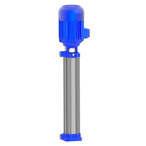
Подъемный насос FH6 для технической воды, охлаждающей жидкости и смазочных материалов
06.10.2024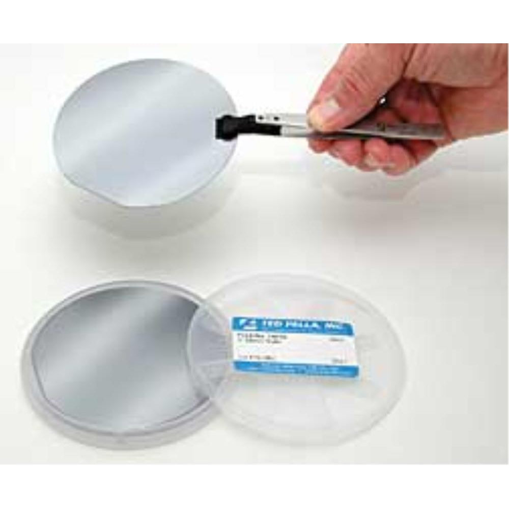
Подложки для кремниевых пластин SEM, тип P, 111
06.10.2024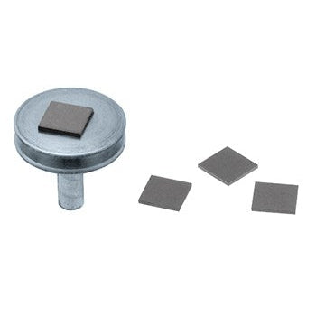
Подкладки АСМ для кремниевых чипов
Зарегистрируйтесь сегодня, и мы отправим вам код на скидку 10% на вашу первую покупку. Применяются некоторые ограничения. Образцы для СЭМ, SIMS, AFM. Они служат гладким, инертным фоном для определения разрешения и контраста СЭМ с возможностью использования ярких электронных излучателей. Кроме того, проводящие образцы или непроводящие образцы…
Подпишитесь сегодня
Sign up today and we will send you a 10% discount code towards your first purchase. Some restrictions apply.
Specimen support for SEM, SIMS, AFM.
They are useful as a smooth, inert background is for the determination of resolution and contrast of in-the-lens SEMs equipped with high brightness electron emitters. Additionally, conducting specimens, or non-conducting specimens in low vacuum or low voltage SEM, may be viewed without coating.
Si chips are opaque, have low electrical resistance, are very smooth, brittle and hard like glass. Si chips are chemically quite inert. These chips are pre-cleaned, but for tissue and cell culture, additional cleaning and sterilising may be required. Si-chips are opaque, of low electrical resistance and have surface properties equal to glass (including smoothness). They are also good substrates for growing or mounting cells. Si-chips are precleaned before packaging. Also ideal for imaging small particles due to low background signal.
The wafers are cut into chips measuring 5 x 5mm, 5 x 7mm, 10 x 10mm or 12 x 12mm.
Технические характеристики
- Orientation: <100>
- Resistance: 1-30 Ohms
- Type: P (Boron) if 1 primary flat
- No SiO2 top coating
- Wafer thickness: 460 – 530um
- Wafer is polished on one side
- Roughness: 2nm
- Before dicing they are rinsed in de-ionized water for cleaning
Peters, K.R., Working at higher magnifications in scanning electron microscopy with secondary and backscattered electrons on metal coated biological specimens and imaging macromolecular cell membrane structures, 1985 Scanning Electron Microscopy, 1985, IV, 159.
Apkarian, R.P., High-resolution signal detection of specimen-specific secondary electrons in an analytical SEM, “Proc. 44th Ann. Meeting of the EMSA”, 1986, G.W. Bailey, Ed., San Francisco Press, 658.
Похожие товары
-
013-4982-2- AMBIENT MIR TGS, УСИЛИТЕЛЬ ПРЕДВАРИТЕЛЬ (EMI)
Запчасти для ремонта
-
0515-0773- ВИНТ-ПРОТИВ ГОЛОВКИ-SKT-HD-CAP M3 X 0,5 6MM
Запчасти для ремонта

